
Nanosecond Wide Bandgap Pulser
Preparation for development of a single stage for a High Power Wide Bandgap nanosecond pulse generator.
Choosing MOSFETs for Consideration
Task 1: Evaluation of Power MOSFETs
The first step in designing a pulse circuit of this magnitude is choosing the correct Wide Band Gap, WBG, MOSFET to use. Due to this, a comparison study of such devices has been made and a board to test these MOSFETs has been designed. The implementation of high voltage (1.7-15kV) MOSFETs has been put into consideration during the design of this test board. A search was made to find the best MOSFET for our situation which involved contacting some WBG MOSFET manufacturers directly. Upon contacting one of these manufacturers, CREE, the packages they had in these voltage ratings consisted of just the bare die package. While implementation of this is possible, the timing of obtaining the package, as well as the implementation onto a board, would take more time and resources than available in the scope of this work. The devices shown in Figure 1 were taken into consideration.


To keep costs down, research was made to decide if it would be possible to design the test board in such a way that all applicable chips could be tested on a single board. Looking at the comparison chart in Figure 1, we see that the silicone, Si, MOSFET has a very long rise time, well outside the scope of a nano-second pulser, and a low Id [2]. This Si MOSFET was a new contender on the market as of the start of this project and therefore was added to the list even though it was not a WBG device. This was done not only to ensure the project was on the correct path, but to validate the overall concept of this project as well. Out of the four 1.7kV MOSFETs, one has a different pin layout that does not match that of the others. The CREE TO-247-4 Plus package comes in a 4-pin package [1].
Figure 1: Table of target transistors [1] [2] [3] [4] [5]
DUT Test-Stand Design
Three key objectives have been focused on throughout the design of the test board and test board circuit. First, the circuit must be able to isolate the drive components from the high voltage components of the project. Second, the circuit must be able to store enough charge to run a significant test of 1 µs or longer. Third, the circuit must act much like the desired final product which means keeping transient spikes at a minimum. Finally, the fourth objective was to design the circuit and board layout in such a way that the driver could easily be replaced with test drivers in order to accomplish task 2 on the test board itself.
The drive component for our design, CRD-001, has been pre-engineered by CREE [6]. It has been designed to accomplish the first of the key objectives as far as the actual gate driver is concerned. As for the rest of the board’s interaction with the gate driver, calculations have been made to ensure proper distances will be maintained [7]. To ensure that the second key objective is met, a calculation has been made to ensure that enough on-board capacitance is available to store the amount of energy needed for this test. The third key objective is actually a very broad objective and will not be covered fully in this report due to the lengthiness of the topic and detail of the calculations made. In general, however, a snubber circuit has been designed whereby experimental values will be used to calculate the proper values for the final test circuit. Also, inductance in the circuit has been kept to a minimum in several ways to ensure fast response and a low amount of ringing. The fourth key objective has been accomplished by using CREE’s pre-engineered CRD-001 gate drive component. Using this as a starting point the inductive drive circuit that is being design for task 2 can be laid in place of the CRD-001. This allows a standard footprint to be used and gives a good point of reference to use for comparison studies.
The circuit design for the gate driver, the power input, and the trigger signal input can be seen in Figure 2. The trigger input will come in through a BNC, Figure 2 top, and chip power supply will be connected via standard power jacks, Figure 2 middle. The bottom circuitry in Figure 2 represents the connection of the CREE gate driver.
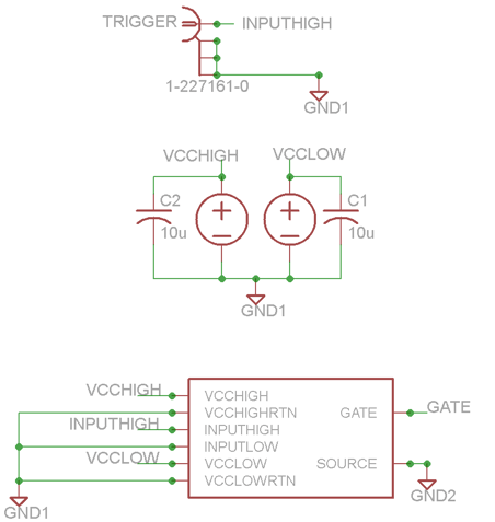
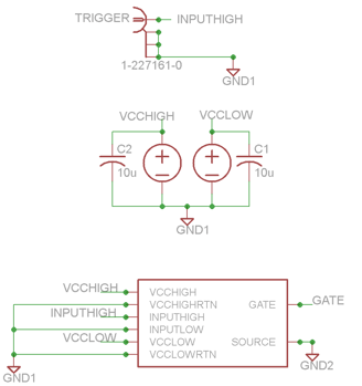
Figure 2: Top and middle, input circuitry, bottom, isolated gate driver
The actual circuit used for this test can be found in Figure 3. The main purpose of this circuit is to test each MOSFET’s current handling capabilities as well as the rise and fall times. This is accomplished by charging the large bank of capacitors with the Device Under Test, DUT, turned off. The DUT is then turned on allowing a discharge of the capacitors. This will give insight into the rise time of the MOSFET if done correctly. The resistor bank is used to limit the overall current that is run through the device. By changing the resistance at this point the current handling capability of the MOSFET can be tested incrementally. The DUT is then turned off before the capacitors are allowed to discharge. This will allow the fall time of the DUT to be tested as well. This whole process, in essence, creates a pulse waveform; however, further design will be needed to fully capture the desired results of the pulse module. The other components in this diagram protect the DUT and keep ringing at a minimum.
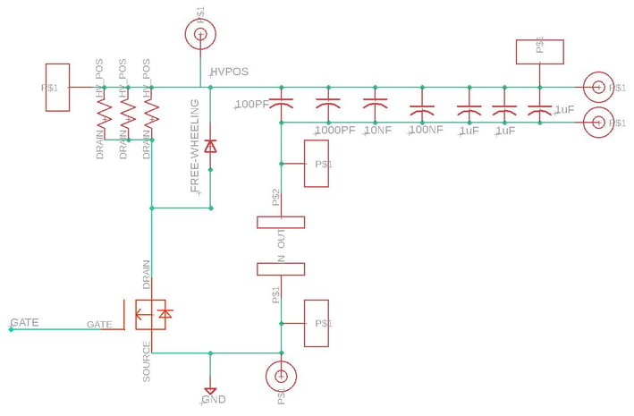
Figure 3: DUT high voltage circuitry
The test green board layout can be found in Figures 4(a), 4(b) and 4(c). Numerous probing points have been designed into the board layout as well as power connection points.
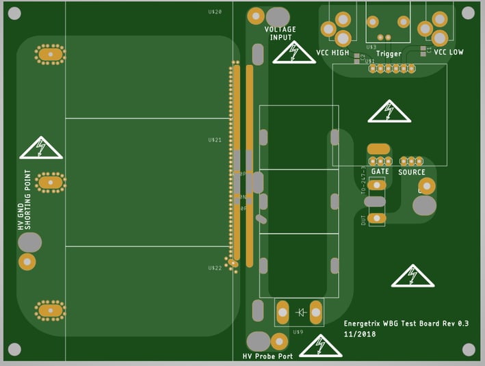
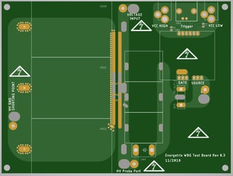
Figure 4(a):Test green board Top PCB layout.

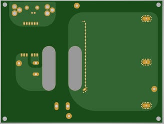
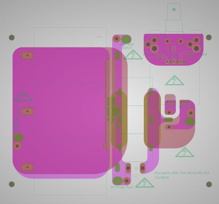
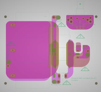
Figure 4(b):Test green board Bottom PCB layout.
Figure 4(c):Test green board PCB layout.
Figure 5 is a picture of the final test board printed, populated and with device under test. This is the test setup used in the rest of this report.
The first two devices tested were the GeneSiC GA08JT17-247 [3] and the ROHM SCT2H12NZ [4]. As suspected, the current handling capability of both devices limited their performance at 1.7 kV with a 10 Ω load, as seen in Figures Figure 6 and Figure 7 (all real time test figures have actual snapshots from the oscilloscope in the ). This limit eliminates these devices from the list of useful high power MOSFETs to be used for this project since they are unable to fully switch the available power from the energy bank into the load. Another criterion that may have warranted further review of these chips is their switching speed. If the switching speed proved to be faster than the other chips, there may have existed a solution for the pulser using these chips.

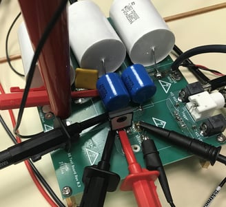
Figure 5: Wide Band Gap MOSFET test board testing C2M0045170D.
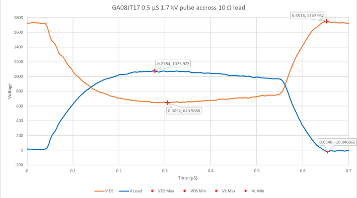
Figure 6: GA08JT17-247 switched into 10 Ohm load, rise time 108.6 ns.
The CREE C2M0045170D proved to be the best SiC MOSFET for this pulse design [5]. Figure 8 shows that the C2M0045170D was able to handle the amount of current produced from the 1.7 kV across itself and the 10 Ω load. Adding to this capability, this MOSFET was able to switch much faster when compared to the other MOSFETs in this test
Test Results
GeneSiC GA08JT17-247 and ROHM SCT2H12NZ
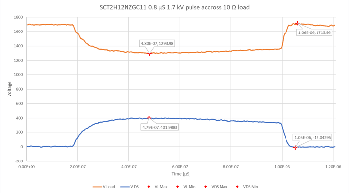
Figure 7: ROHM SCT2H12NZGC11 switched into 10 Ω load, rise time 97.2 ns. (**NOTE in print, the values for V Load and V DS were swapped, the blue line is V Load and the Orange line is V DS**)
CREE C2M0045170D
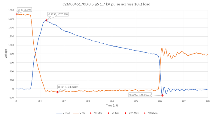
Figure 8:CREE C2M0045170D switched into 10 Ω load, rise time of 54.8 ns
To get a feel for how this MOSFET will perform in the final pulse circuit, a test was run with a 65 ns trigger pulse. The results for this pulse can be seen in Figure 9 (this pulse is more impressive seen in the appendix, Figure 17). The CREE C2M0045170D will be used in the design for the final pulsing circuit.
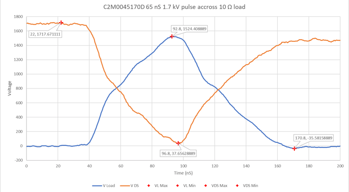
Figure 9: CREE C2M0045170D switched into 10 Ω load, rise time of 41.7 ns
Task 2: Device Package Limitations
Inductive Drive Design and Simulation
The final pulse design will need faster switching than that which is capable using the CRD-001. Task 2 of this project focuses on device package design, namely the high parasitic inductance inherent standard device packaging techniques. This high parasitic inductance slows switching speeds directly due to the limited amount of di/dt available to charge the gate. A decision to focus in the area that can garner the most gains in switching speed has been made. This area of focus is in the driver design. An inductive drive system has been designed based on the work of Landon Collier and his team [8]. The author of this deliverables report did some work on this design with Mr. Collier during the authors time as an undergraduate including making a simulation circuit and detailing design plans. The basic design for the inductive drive can be seen in Figure 10.
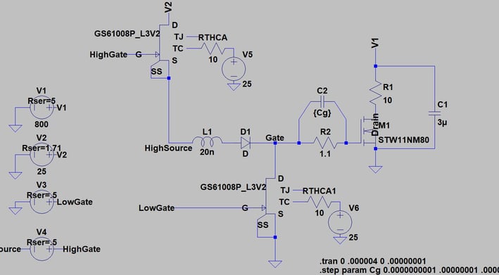
Figure 10: Inductive drive simulation circuit.
In this design, energy is built up in the inductor, L1, via current flow through the upper and lower switches, GS61008P, to ground. The lower switch is then turned off and the energy built up in the inductor, having nowhere to go, creates a voltage spike on the “Gate” node. This voltage spike would normally be damaging to the MOSFET but the internal parasitics of the MOSFET take the bulk of the initial drop. As this spike is happening current rushes into the gate of the MOSFET increasing charge on the device, ultimately turning it on. Eventually the voltage drops to its nominal value, determined by V2, and the device is held on by the built-up charge. At this point the high side switch is turned off followed by the low side switch which allows the gate charge to drain to ground; thereby turning off the MOSFET. The high side switch can then be turned on to start the process again. The waveforms of this whole process, not including the V(DS) of the DUT, can be seen in Figures Figure 11 and Figure 12.
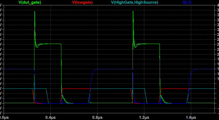
Figure 11: All in one snapshot of the nodes in the circuit of Figure 10.
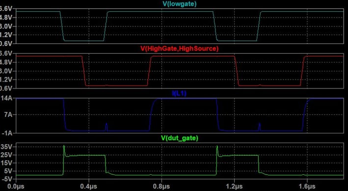
Figure 12: Side by side snapshot of the nodes in the circuit of Figure 10.
Inductive Drive Circuit internal MOSFETs and Drivers.
The parts and general layout for the inductive drive system have been selected using various sources [9] [10]. Figure 13 shows a basic block diagram of the gate drive circuit including part numbers for those found thus far. A single isolated design has been chosen for both the high side and low side GaN FET drivers allowing ease of design and implementation. Starting from the top left of the figure in the “High Side” area, a DC/DC converter, RKZE-2409, was chosen that could supply the system with 9 V using a 24 V input [11]. Calculations were made to ensure that the 2 W RKZE-2409 would be able to provide ample power to each GaN driver system, which use approximately 700 mW. Moving to the right of the DC/DC converter, the LP2985AIM Low Dropout regulator, LDO, has been chosen to supply power to the GaN side of the gate driver system [12]. Caddy corner to the LDO, below the DC/DC converter, the Optocoupler chosen for this design, HCNW 4506, will be used to isolate the trigger source from the drive circuit [13]. The single-channel high-speed gate driver chosen for this design, UCC27511A, has been chosen for its unique capability of driving GaN FET’s without tripping its UVLO [14]. This driver will drive the GaN Systems GS61008P through a resistor network [15]. The high side FET connects to the high current capable energy storage circuit and the inductor. Three separate inductor kits, C302, C308, and C318, have been chosen for this design due to the need to experimentally choose the proper energy storage after the driver board has been printed and populated [16]. At the time of this writing not all parts have been chosen. Those blocks in the diagram that are missing part numbers will need to be chosen, besides the SiC MOSFET which has been chosen by the previous testing found in this paper. As previously mentioned, the low side drive components match that of the high side.
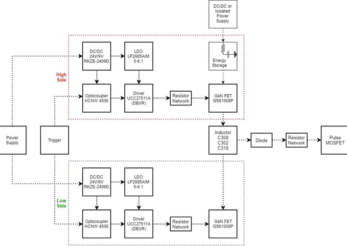
Figure 13: GaN based inductive drive block diagram with part numbers.
References
[1] CREE, "C2M0080170P Silicon Carbide Power MOSFET C2M MOSFET Technology.," 05 2018. [Online]. Available: https://www.mouser.com/catalog/specsheets/Cree-05-18-2018-C2M0080170P.pdf. [Accessed 1 7 2018].
[2] IXYS, "High Voltage Power MOSFET," 2013. [Online]. Available: http://ixapps.ixys.com/datasheet/ds100458b(ixtl2n450).pdf. [Accessed 5 7 2018].
[3] GeneSiC, "Normally - OFF Silicone Carbide Junction Transistor," 2014. [Online]. Available: http://www.genesicsemi.com/images/products_sic/sjt/GA08JT17-247.pdf. [Accessed 3 7 2018].
[4] ROHM, "N-Channel SiC power MOSFET," 2015. [Online]. Available: https://www.rohm.com/datasheet/SCT2H12NZ/sct2h12nz-e. [Accessed 2 7 2018].
[5] Cree, "Cree C2M0045170D," 06 2016. [Online]. Available: http://www.wolfspeed.com/media/downloads/886/C2M0045170D.pdf. [Accessed 1 2017].
[6] Cree, "SiC MOSFET Isolated Gate Driver," Cree, 2014. [Online]. Available: http://www.wolfspeed.com/media/downloads/572/CPWRAN10.pdf . [Accessed 1 2017].
[7] R. Tarzwell and K. Bahl, "High Voltage Printed Circuit Design & Manufacturing Notebook," 2004.
[8] T. K. J. D. J. M. A. N. L. Collier, "An Inductive Gate Drive Approach to Fast SiC," IEEE TRANSACTIONS ON POWER ELECTRONICS, pp. 2-7, n.d..
[9] GaN Systems, "Design with GaN Enhancement mode HEMT," 28 2 2018. [Online]. Available: https://gansystems.com/wp-content/uploads/2018/02/GN001_Design_with_GaN_EHEMT_180228-1.pdf. [Accessed 15 4 2019].
[10] B. Maurice and L. Wuidart, "Drive Circuits For Power MOSFETs and IGBTs," STMicroelectronics, 1999. [Online]. Available: http://www.st.com/content/ccc/resource/technical/document/application_note/68/cd/c6/ab/ef/17/41/06/CD00003900.pdf/files/CD00003900.pdf/jcr:content/translations/en.CD00003900.pdf. [Accessed 1 2017].
[11] Recom, "RKZE 2 Watt SIP7 Single and Dual Output," 2018. [Online]. Available: https://www.mouser.com/datasheet/2/468/RKZE-1369815.pdf. [Accessed 15 4 2019].
[12] Texas Instruments Incorperated, "LP2985-N Micropower 150 mA Low-Noise Ultra-Low-Dropout Regulator in a SOT-23 Package Designed for Use With Very Low ESR Output Capacitors," 12 2016. [Online]. Available: http://www.ti.com/lit/ds/symlink/lp2985-n.pdf. [Accessed 15 4 2019].
[13] Avago Technologies, "HCPL-4506/J456/0466, HCNW4506 Intelligent Power Module and Gate Drive Interface Optocouplers," 10 7 2007. [Online]. Available: https://datasheet.octopart.com/HCPL-4506-Avago-datasheet-7552030.pdf. [Accessed 14 4 2019].
[14] Texas Instruments Incorperated, "UCC27511A Single-Channel High-Speed Low-Side Gate Driver," 2018. [Online]. Available: http://www.ti.com/lit/ds/symlink/ucc27511a.pdf?HQS=TI-null-null-mousermode-df-pf-null-wwe&DCM=yes&ref_url=https%3A%2F%2Fwww.mouser.com%2F. [Accessed 16 4 2019].
[15] GaN Systems Inc., "GS61008P Bottom-side cooled 100 V E-mode GaN transistor Preliminary Datasheet," 2018. [Online]. Available: https://www.mouser.com/datasheet/2/692/GS61008P-DS-Rev-180213-1314185.pdf. [Accessed 13 4 2019].
[16] Coilcraft, "Magnetics for RF, power, filter and data applications," 4 2018. [Online]. Available: https://www.mouser.com/datasheet/2/597/ShortFormCatalog-934560.pdf. [Accessed 17 4 2019].
[17] L. T. B. Ozpineci, "COMPARISON OF WIDE-BANDGAP SEMICONDUCTORS FOR POWER ELECTRONICS APPLICATIONS," 12 12 2003. [Online]. Available: https://pdfs.semanticscholar.org/adc4/3f685e660d2033eafcbcca80295a3f7aafe0.pdf. [Accessed 15 01 2019].
[18] M. D. Sheburn, "Design of a 15MW Solid-State Linear Transformer Driver for Gas Switch Triggering Applications," 2 5 2018. [Online]. Available: https://vtechworks.lib.vt.edu/bitstream/handle/10919/83932/Sherburne_MD_T_2018.pdf?sequence=1&isAllowed=y. [Accessed 10 1 2019].
Appendix
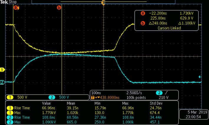
Figure 14: Actual oscilloscope reading, GeneSiC GA08JT17-247 with 10 Ohm load. Blue represents voltage across the load and yellow represents drain to source voltage.
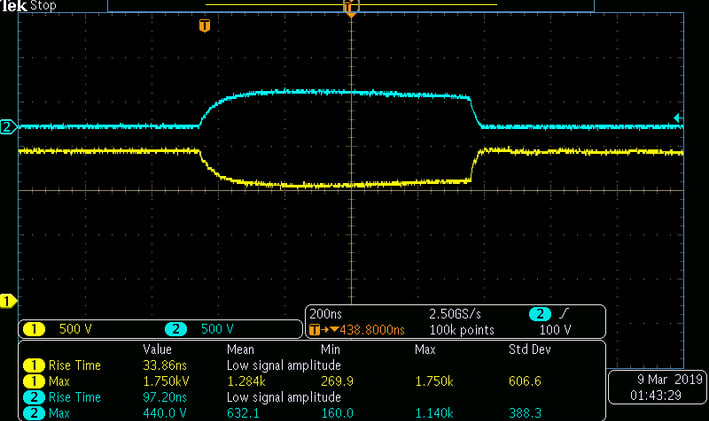
Figure 15: Actual oscilloscope reading, ROHM SCT2H12NZGC11 with 10 Ohm load. Blue represents voltage across the load and yellow represents drain to source voltage.
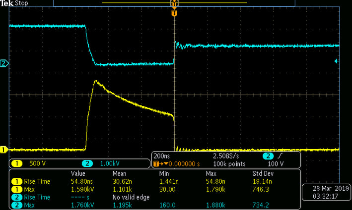
Figure 16: Actual oscilloscope reading, CREE C2M0045170D with 10 Ohm load. Yellow represents voltage across the load and blue represents drain to source voltage, 500 ns pulse.
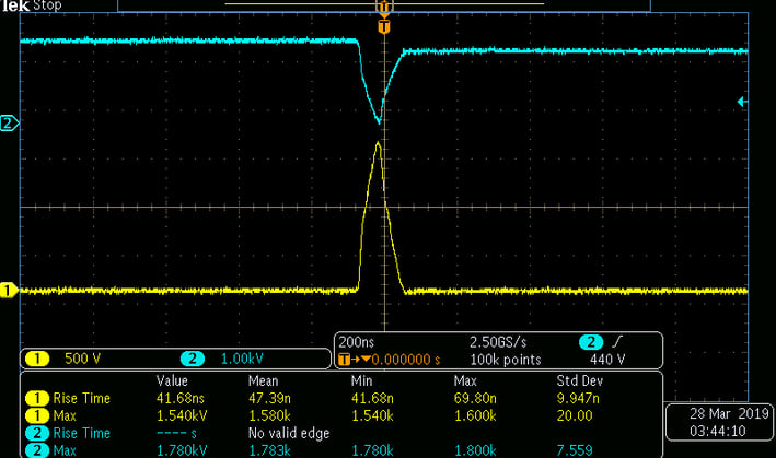
Figure 17: Actual oscilloscope reading, CREE C2M0045170D with 10 Ohm load. Yellow represents voltage across the load and blue represents drain to source voltage, 65 ns pulse.


